
This design is derived from the portable Headphone Ampliflier featuring an NPN/PNP compound pair emitter follower output stage. An improved output driving capability is gained by making this a push-pull Class-A arrangement. Output power can reach 427mW RMS into a 32 Ohm load at a fixed standing current of 100mA.
The single voltage gain stage allows the easy implementation of a shunt-feedback circuitry giving excellent frequency stability.
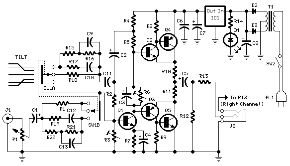
Parts:
P1_____________22K Dual gang Log Potentiometer (ready for Stereo)
R1_____________15K 1/4W Resistor
R2____________220K 1/4W Resistor
R3____________100K 1/2W Trimmer Cermet
R4_____________33K 1/4W Resistor
R5_____________68K 1/4W Resistor
R6_____________50K 1/2W Trimmer Cermet
R7_____________10K 1/4W Resistor
R8,R9__________47K 1/4W Resistors
R10,R11_________2R2 1/4W Resistors
R12_____________4K7 1/4W Resistor
R13_____________4R7 1/2W Resistor
R14_____________1K2 1/4W Resistor
R15,R18_______330K 1/4W Resistors (Optional)
R16___________680K 1/4W Resistor (Optional)
R17,R19_______220K 1/4W Resistors (Optional)
R20,R21________22K 1/4W Resistors (Optional)
C1,C2,C3,C4____10µF 25V Electrolytic Capacitors
C5,C7_________220µF 25V Electrolytic Capacitors
C6,C11________100nF 63V Polyester Capacitors
C8___________2200µF 25V Electrolytic Capacitor
C9,C12__________1nF 63V Polyester Capacitors (Optional)
C10___________470pF 63V Polystyrene or Ceramic Capacitor (Optional)
C13____________15nF 63V Polyester Capacitor (Optional)
D1_____________5mm. or 3mm. LED
D2,D3________1N4002 100V 1A Diodes
Q1,Q2_________BC550C 45V 100mA Low noise High gain NPN Transistors
Q3____________BC560C 45V 100mA Low noise High gain PNP Transistor
Q4____________BD136 45V 1.5A PNP Transistor
Q5____________BD135 45V 1.5A NPN Transistor
IC1____________7815 15V 1A Positive voltage regulator IC
T1_____________220V Primary, 15 + 15V Secondary (30V center-tapped)
5VA Mains transformer
SW1____________4 poles 3 ways rotary Switch (ready for Stereo)
SW2____________SPST slide or toggle Switch
J1_____________RCA audio input socket
J2_____________6mm. or 3mm. Stereo Jack socket
PL1____________Male Mains plug
Notes:
* Q4, Q5 and IC1 must be fitted with a small U-shaped heatsink.
* For a Stereo version of this circuit, all parts must be doubled except P1, IC1, R14, D1, D2, D3, C8, T1, SW1, SW2, J2 and PL1.
* If the Tilt Control is not needed, omit SW1, all resistors from R15 onwards and all capacitors from C9 onwards. Connect the rightmost terminal of R1 to the Base of Q1.
* Before setting quiescent current rotate the volume control P1 to the minimum, Trimmer R6 to zero resistance and Trimmer R3 to about the middle of its travel.
* Connect a suitable headphone set or, better, a 33 Ohm 1/2W resistor to the amplifier output.
* Connect a Multimeter, set to measure about 10Vdc fsd, across the positive end of C5 and the negative ground.
* Switch on the supply and rotate R3 in order to read about 7.7-7.8V on the Multimeter display.
* Switch off the supply, disconnect the Multimeter and reconnect it, set to measure at least 200mA fsd, in series to the positive supply of the amplifier.
* Switch on the supply and rotate R6 slowly until a reading of about 100mA is displayed.
* Check again the voltage at the positive end of C5 and readjust R3 if necessary.
* Wait about 15 minutes, watch if the current is varying and readjust if necessary.
* Those lucky enough to reach an oscilloscope and a 1KHz sine wave generator, can drive the amplifier to the maximum output power and adjust R3 in order to obtain a symmetrical clipping of the sine wave displayed.
Technical data:
Output power (1KHz sinewave):
32 Ohm: 427mW RMS
64 Ohm: 262mW RMS
100 Ohm: 176mW RMS
300 Ohm: 64mW RMS
600 Ohm: 35mW RMS
2000 Ohm: 10mW RMS
Sensitivity:
140mV input for 1V RMS output into 32 Ohm load (31mW)
500mV input for 3.5V RMS output into 32 Ohm load (380mW)
Frequency response @ 2V RMS:
See the above graph
Total harmonic distortion into 32 Ohm load @ 1KHz:
1V RMS 0.005% 3V RMS 0.015% 3.65V RMS (onset of clipping) 0.018%
Total harmonic distortion into 32 Ohm load @ 10KHz:
1V RMS 0.02% 3V RMS 0.055% 3.65V RMS (onset of clipping) 0.1%
The single voltage gain stage allows the easy implementation of a shunt-feedback circuitry giving excellent frequency stability.
Parts:
P1_____________22K Dual gang Log Potentiometer (ready for Stereo)
R1_____________15K 1/4W Resistor
R2____________220K 1/4W Resistor
R3____________100K 1/2W Trimmer Cermet
R4_____________33K 1/4W Resistor
R5_____________68K 1/4W Resistor
R6_____________50K 1/2W Trimmer Cermet
R7_____________10K 1/4W Resistor
R8,R9__________47K 1/4W Resistors
R10,R11_________2R2 1/4W Resistors
R12_____________4K7 1/4W Resistor
R13_____________4R7 1/2W Resistor
R14_____________1K2 1/4W Resistor
R15,R18_______330K 1/4W Resistors (Optional)
R16___________680K 1/4W Resistor (Optional)
R17,R19_______220K 1/4W Resistors (Optional)
R20,R21________22K 1/4W Resistors (Optional)
C1,C2,C3,C4____10µF 25V Electrolytic Capacitors
C5,C7_________220µF 25V Electrolytic Capacitors
C6,C11________100nF 63V Polyester Capacitors
C8___________2200µF 25V Electrolytic Capacitor
C9,C12__________1nF 63V Polyester Capacitors (Optional)
C10___________470pF 63V Polystyrene or Ceramic Capacitor (Optional)
C13____________15nF 63V Polyester Capacitor (Optional)
D1_____________5mm. or 3mm. LED
D2,D3________1N4002 100V 1A Diodes
Q1,Q2_________BC550C 45V 100mA Low noise High gain NPN Transistors
Q3____________BC560C 45V 100mA Low noise High gain PNP Transistor
Q4____________BD136 45V 1.5A PNP Transistor
Q5____________BD135 45V 1.5A NPN Transistor
IC1____________7815 15V 1A Positive voltage regulator IC
T1_____________220V Primary, 15 + 15V Secondary (30V center-tapped)
5VA Mains transformer
SW1____________4 poles 3 ways rotary Switch (ready for Stereo)
SW2____________SPST slide or toggle Switch
J1_____________RCA audio input socket
J2_____________6mm. or 3mm. Stereo Jack socket
PL1____________Male Mains plug
Notes:
* Q4, Q5 and IC1 must be fitted with a small U-shaped heatsink.
* For a Stereo version of this circuit, all parts must be doubled except P1, IC1, R14, D1, D2, D3, C8, T1, SW1, SW2, J2 and PL1.
* If the Tilt Control is not needed, omit SW1, all resistors from R15 onwards and all capacitors from C9 onwards. Connect the rightmost terminal of R1 to the Base of Q1.
* Before setting quiescent current rotate the volume control P1 to the minimum, Trimmer R6 to zero resistance and Trimmer R3 to about the middle of its travel.
* Connect a suitable headphone set or, better, a 33 Ohm 1/2W resistor to the amplifier output.
* Connect a Multimeter, set to measure about 10Vdc fsd, across the positive end of C5 and the negative ground.
* Switch on the supply and rotate R3 in order to read about 7.7-7.8V on the Multimeter display.
* Switch off the supply, disconnect the Multimeter and reconnect it, set to measure at least 200mA fsd, in series to the positive supply of the amplifier.
* Switch on the supply and rotate R6 slowly until a reading of about 100mA is displayed.
* Check again the voltage at the positive end of C5 and readjust R3 if necessary.
* Wait about 15 minutes, watch if the current is varying and readjust if necessary.
* Those lucky enough to reach an oscilloscope and a 1KHz sine wave generator, can drive the amplifier to the maximum output power and adjust R3 in order to obtain a symmetrical clipping of the sine wave displayed.
Technical data:
Output power (1KHz sinewave):
32 Ohm: 427mW RMS
64 Ohm: 262mW RMS
100 Ohm: 176mW RMS
300 Ohm: 64mW RMS
600 Ohm: 35mW RMS
2000 Ohm: 10mW RMS
Sensitivity:
140mV input for 1V RMS output into 32 Ohm load (31mW)
500mV input for 3.5V RMS output into 32 Ohm load (380mW)
Frequency response @ 2V RMS:
See the above graph
Total harmonic distortion into 32 Ohm load @ 1KHz:
1V RMS 0.005% 3V RMS 0.015% 3.65V RMS (onset of clipping) 0.018%
Total harmonic distortion into 32 Ohm load @ 10KHz:
1V RMS 0.02% 3V RMS 0.055% 3.65V RMS (onset of clipping) 0.1%


Tidak ada komentar:
Posting Komentar